18th February 2026
 https://www.allpsu.co.uk/wp-content/uploads/2026/02/EC3AW8-EC4AW8-500x325.jpeg EC3AW8-EC4AW8
How can we help?

Please get in touch using the form below.
by Jenny Olding |
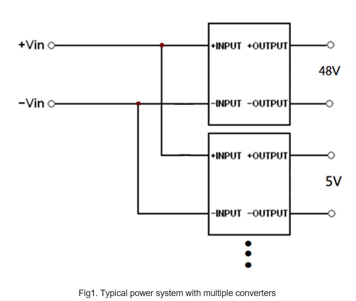
In some applications, different supply voltages would be applied for powering different types of function in a system. For example, a modern telecom system may use at least two supply rails: one is to power the telecom device, and the other one with the lower supply voltage is to power the microprocessor. These supply voltages may be generated by voltage regulators or DC-DC converters. If the system has multiple DC-DC converters for the different voltage supply rails, it will require a mechanism to minimize the switching noise distributed in the power distribution network of the system. This ripple & noise is usually reduced by adding the external decoupling capacitors at the input and output sides of the DC-DC converters. However, different switching frequencies of the DC-DC converters may bring the additional challenge to solve the EMI issue for the entire power system. In that case, the Sync Pin would be helpful to solve the problem.
The switching frequency of CHB150W12 & CHB200W12 series can be synchronized with frequency of an external clock by giving a narrow pulse to the DC-DC converter via the Sync pin. The setup for the Sync function is shown as below:
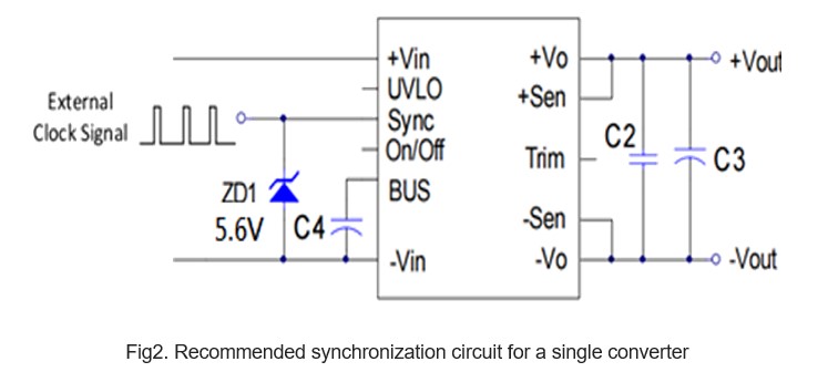
The specifications of synchronization signal are the same for CHB150W12 and CHB200W12 series. In addition, the signal should be a TTL (Transistor-Transistor Logic) compatible signal with a maximum amplitude of 5.6V to prevent damage to the input pin of synchronization.
Note:
The frequency of the external clock must be between 530KHz~630KHz.
The pulse width of the external clock must be between 75ns ~ 120ns.
The voltage at the Sync pin must be driven to exceed 3.5V ~ 4.5V level.
If the external clock frequency is less than the switching frequency of CHB150W12 and CHB200W12, the module will ignore the pulse from the sync pin.
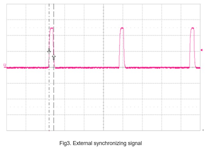
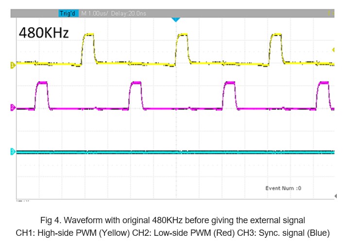
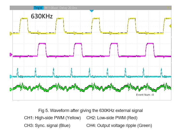
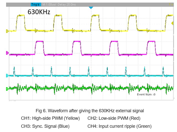
We could find that the original switching frequency of CHB150W12 and CHB200W12 is 480Khz from the waveform (Fig 4). After giving the external signal through sync pin, the PWM waveform is synchronized to be 630Khz. Moreover, it shows the output voltage ripple and Input current ripple could be synchronized as well (Fig 5 & 6).
 The following block diagram (Fig7.) shows two DC-DC converters that have the sync function. They are on the same input bus and a signal would come from an external source of signal to synchronize both converters with the same switching frequency.
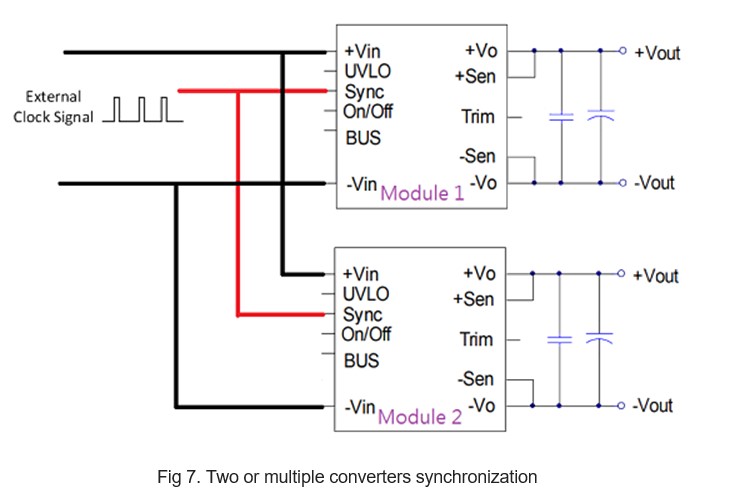
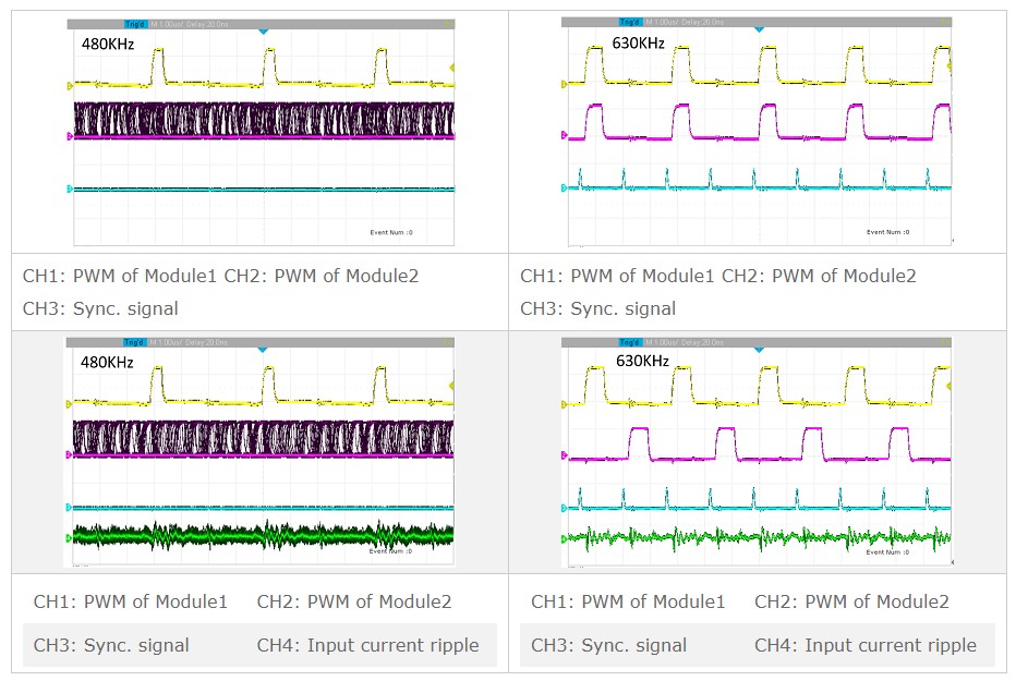
According to the waveforms above, while the trigger is set to the PWM of Module 1 on the oscilloscope, the waveform of PWM is clearly shown. Furthermore, the persistence setting makes the waveform of PWM of Module 2 blurry, meaning the switching frequency is not completely the same as the that of Module 1. After the synchronization with 630KHz, the PWM waveform of converter 2 is clearly shown as well. Both Modules could operate at the same frequency and turn on their switches at the same time.
Via the brief demonstration of synchronizing single and two converters, technically speaking, the process of synchronization not only solves the problem of interference resulted from different switching frequency in a system but also reduces the input ripple current and output ripple voltage on paralleling more modules. This is like the concept of multi-phase interleaving.
We provide CHB150W12 and CHB200W12 DC-DC converter series which could offer the function of synchronizing the switching frequency. Through an external signal, these converters could be synchronized with the same switching frequency and the input ripple current and output ripple voltage could be moderated. For more information, please check the product page or contact us for support.
https://www.allpsu.co.uk/wp-content/uploads/2026/02/EC3AW8-EC4AW8-500x325.jpeg EC3AW8-EC4AW8 https://www.allpsu.co.uk/wp-content/uploads/2021/11/arcv60-500x378.jpg arcv60-encapsulated-power-supply
 https://www.allpsu.co.uk/wp-content/uploads/2026/02/CFM600S-500x336.jpg CFM600S